Any microcontroller board is a PCB that have connections made to the pins of a microcontroller chip. A microcontroller chip is ready to go if it has a power supply, a ground connection, an oscillator and a reset pin.
So before making connections of uC pins on a board, we should know what different pins are meant for.
***************************
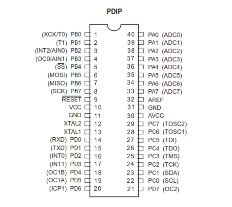
Pin Descriptions (*from data sheet)
Pin 10- VCC Digital supply voltage.
Pin 32- GND Ground.
Port A (PA7-PA0) Port A serves as the analog inputs to the A/D Converter.
Port A also serves as an 8-bit bi-directional I/O port, if the A/D Converter is not used. Port pins can provide internal pull-up resistors (selected for each bit). The Port A output buffers have symmetrical drive characteristics with both high sink and source capability. When pins PA0 to PA7 are used as inputs and are externally pulled low, they will source current if the internal pull-up resistors are activated.
The Port A pins are tri-stated when a reset condition becomes active, even if the clock is not running.
Port B (PB7-PB0) Port B is an 8-bit bi-directional I/O port with internal pull-up resistors (selected for each bit). The Port B output buffers have symmetrical drive characteristics with both high sink and source capability. As inputs, Port B pins that are externally pulled low will source current if the pull-up resistors are activated. The Port B pins are tri-stated when a reset condition becomes active, even if the clock is not running. Port B also serves the functions of various special features of the ATmega16.
Port C (PC7-PC0) Port C is an 8-bit bi-directional I/O port with internal pull-up resistors (selected for each bit). The Port C output buffers have symmetrical drive characteristics with both high sink and source capability. As inputs, Port C pins that are externally pulled low will source current if the pull-up resistors are activated. The Port C pins are tri-stated when a reset condition becomes active, even if the clock is not running. If the JTAG interface is enabled, the pull-up resistors on pins PC5(TDI), C3(TMS) and PC2(TCK) will be activated even if a reset occurs.
Port C also serves the functions of the JTAG interface and other special features of the ATmega16.
Port D (PD7-PD0) Port D is an 8-bit bi-directional I/O port with internal pull-up resistors (selected for each bit). The Port D output buffers have symmetrical drive characteristics with both high sink and source capability. As inputs, Port D pins that are externally pulled low will source current if the pull-up resistors are activated. The Port D pins are tri-stated when a reset condition becomes active, even if the clock is not running. Port D also serves the functions of various special features of the ATmega16.
RESET – Reset Input. A low level on this pin for longer than the minimum pulse length will generate a reset, even if the clock is not running. Shorter pulses are not guaranteed to generate a reset.
XTAL1 Input to the inverting Oscillator amplifier and input to the internal clock operating circuit. XTAL2 Output from the inverting Oscillator amplifier.
AVCC – AVCC is the supply voltage pin for Port A and the A/D Converter. It should be externally connected to VCC, even if the ADC is not used. If the ADC is used, it should be connected to V through a low-pass filter.
AREF – AREF is the analog reference pin for the A/D Converter.
*********************************
So in brief all pin have some of other function attached to it other than being simply Input or output. This is specifically the register attached to that pin which when activated or set HIGH or ON by writing on particular registers, performs the particular task.
Oscillator is connected to XTAL1 and XTAL2.
Ground is connected to pin 32 and VCC to pin 10.
AVCC is shorted to VCC.
AREF is also given 5V supply.
RESET is active LOW pin. If a 0 volt signal is given when input power is also HIGH, the code in uC restarts.
We also want that at every time we start our uC, it starts with a reset. So a capacitor is connected to RESET pin. So when power is supplied to board, uC is ON but reset is LOW as it takes some to time to charge and reach 5V level. So it RESET’s on every start. A switch is also connected that is grounded and connected to RESET, so when it is pressed, capacitor discharges and it RESET’s.
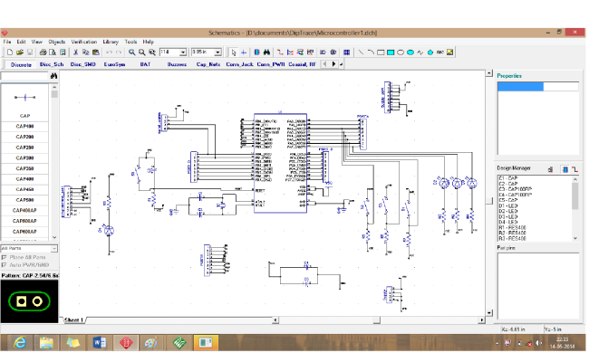
Schematic for a simple microcontroller board is here below:
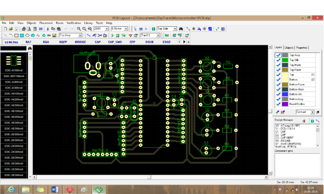
And its PCB layout:
Above circuit connects Port A, B, C and D with a port pattern.
PORT A further have LED’s and switches connected via resistors.
Another important circuit is the Programming Port! It is port having MISO, MOSI, SCK, RESET, VCC and Ground. Through this a programmer is connected via which code is written from computer to uC made possible by communication set between the uC and PC through another uC in Programmer.
Oscillator pins are severely affected by noise signals so they are kept as near to uC as possible. Two capacitors are connected to input and output of oscillator and other end is grounded. Note that the circuit for oscillator is already present in uC but due to fabrication limitations we need to connect to it externally.
Power port is also important to connect peripherals to boards and power and ground them.
To end the blog I would mention about the Arduino board and similar boards. These are ready made platform and are very reliable as connections are precise. The board do not require a programmer to write a code in it. For this purpose a part of memory of uC is dedicated and Bootloader is programmed to run every time you write a code.
This makes it free from external uC to help it communicate with the computer.
Thanks for reading!


